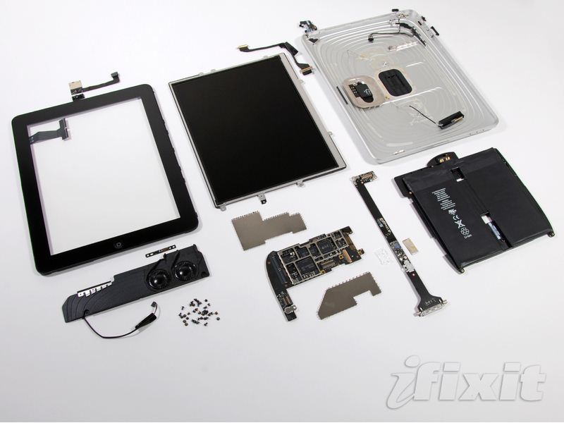
Say, did you get yourself a sleeky Apple iPad today, or are you one of those people who prefer waiting for internal components to first show up and then make a decision? If you got it already, congrats, otherwise you won’t have to wait that long, because the FCC people, that apparently do their job day and night, have completely teared down in pieces the latest and greatest Apple wonder just for you – and boy it looks HOT. Still, no nitty gritty details about the kind of chips and some other parts that make this tablet work so fast and load up things in a snap (although we do know about this Apple 1GHz A4 chipset). Having said that, you know, it’s just a matter of time until those internal specs break cover, courtesy of the iFixit chaps.
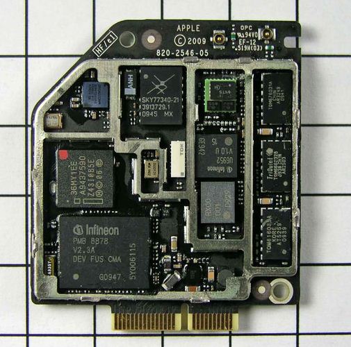
Update: The iFixit fellows have done it again. Here’s their tear down roundup: Apparently, the iPad’s memory is hidden inside this customized A4 processor which looks to be manufactured by Samsung. The battery itself which appears to be 5.5x stronger than any iPhone battery is big (a 3.75V, 24.8 watt-hour at 148 grams) and assembled from two separate batteries (cell mark: P11GA6-01-C01F and 741-00310A +) wired in parallel. On average use it appears that Apple has created a very economical machine that uses only 2.5 Watts, while the chassis is made of environmental-friendly recyclable aluminum and glass materials, free of PVC, BFR, Mercury or Arsenic poisonous metalloid. And speaking about glass, the iPad touchscreen panel is pretty thick, around 1.18 mm, compared to the 1.02 mm you’ll find in the iPhone. The hidden rumored compartment we thought that Apple would use for a built-in webcam turns to be an ambient light sensor slot and the empty void in the upper right corner belongs to the cellular communications board you’ll only find inside the 3G iPad. Display and rear case assembly are 350g each, which makes your iPad fairly ergonomic and balanced, while logic board is about 4.5″ wide, spanning about 60% of the iPad’s width. GPS is notably lacking from the RF/data cable (in non 3G iPads), but the 802.11n WiFi/Bluetooth Broadcom card is well integrated into the dock connector cable. Another image of the 3G component is right after the break.
[via iFixit]


Comments are closed.